Universal PWM Controller terminal connections

Connectors :

P1 connects to the PC parallel port.

P3 and J3 connect to the encoders. You have your choice of the IDC punch-down connectors or the ribbon-cable connector. Note that +5 V power and ground are only available on J3. If using P3, then Encoder power and ground can be taken from P2. For each axis, the encoder signals are A, B and Z, if used. If there is no Z channel on the encoder, then connect the A output to both A and Z, to provide a repeatable signal on the Z input to enable home detection. Pins are as follows :
Pin # Board Marking Signal
1 A0 Axis 0 A
2 B0 Axis 0 B
3 Z0 Axis 0 Z (index)
4 A1 Axis 1 A
5 B1 Axis 1 B
6 Z1 Axis 1 Z (index)
7 A2 Axis 2 A
8 B2 Axis 2 B
9 Z2 Axis 2 Z (index)
10 A3 Axis 3 A
11 B3 Axis 3 B
12 Z3 Axis 3 Z (index)
13 Ground
14 + 5 V

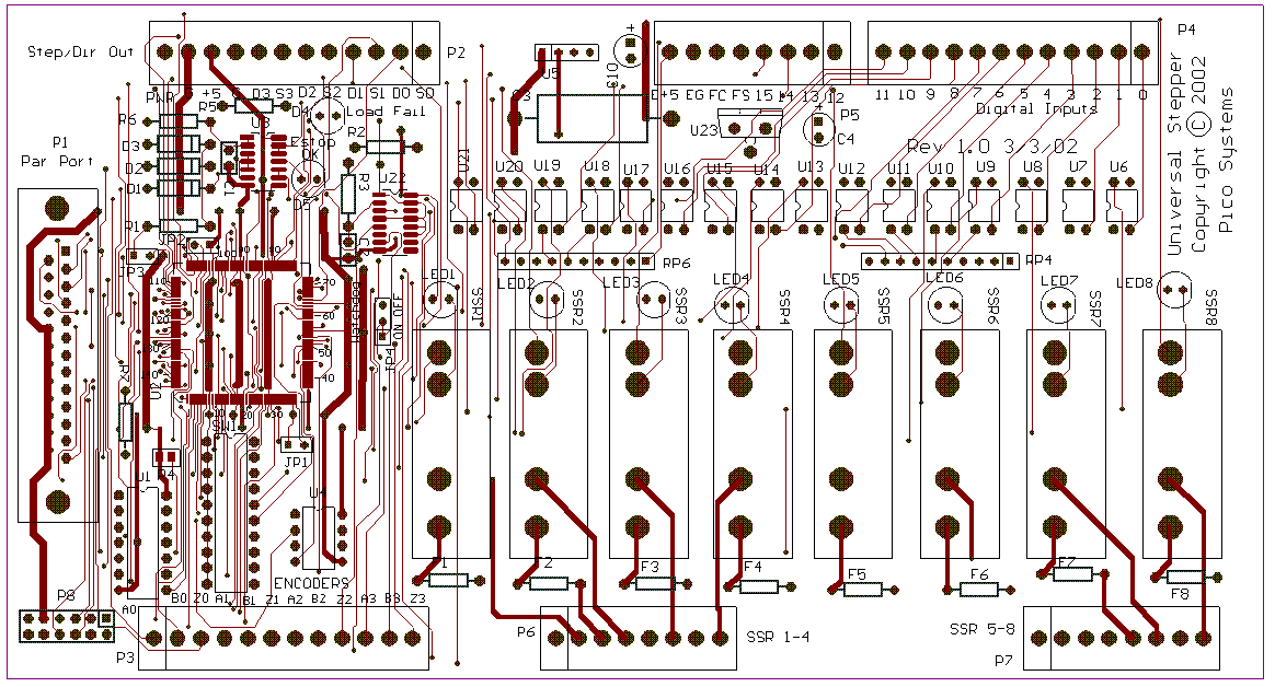
P2 connects to the PWM amplifiers, and also provides unregulated power to the board, and regulated +5 V can be taken from the board to supply encoders. J2 parallels the connections available on P2 except for the unregulated power input. The PWM signal is zero Volts for "power off" and 5 V for "power on". The driving software could make the PWM waveform operate in the inverted manner, but the E-stop condition will always default to zero Volts. If driving opto-coupled amplifier inputs, connect the + amplifier input terminal to pin 3 (+5 V) and the - input to the PWM or direction pin. If this connection is the wrong polarity, and the amp cannot be switched to invert the sense of the PWM or direction inputs, then you can connect the + to the PWM or direction output and the - input to pin 4 (ground). This should still give sufficient current drive to most opto-couplers. Pins are as follows :
P2 Pin # J2 Pin # Board Marking Signal
1 1 S0 PWM to Axis 0
2 2 D0 Direction to Axis 0
3 3 S1 PWM to Axis 1
4 4 D1 Direction to Axis 1
5 5 S2 PWM to Axis 2
6 6 D2 Direction to Axis 2
7 7 S3 PWM to Axis 3
8 8 D3 Direction to Axis 3
9 13 G power ground (same as P2-11)
10 14 +5 +5 Volt output
11 G power ground
12 PWR Unregulated power in

P4 and P5 connect to the digital input contact closures, and also provide isolated +5 V power for these switches. J4 brings out the same connections in ribbon cable header form. P5-7 and P5-8 are a source of isolated 5 V power from an on-board DC-DC converter, to be used for the digital inputs. For each input, a switch is connected between that input and P5-7. P4 Pins are as follows :
P4 Pin # J4 Pin # Board Marking Signal Function
1 1 0 Bit 0 input X Home
2 2 1 Bit 1 input -X Limit
3 3 2 Bit 2 input +X Limit
4 4 3 Bit 3 input available
5 5 4 Bit 4 input Y Home
6 6 5 Bit 5 input -Y Limit
7 7 6 Bit 6 input +Y Limit
8 8 7 Bit 7 input available
9 9 8 Bit 8 input Z Home
10 10 9 Bit 9 input -Z Limit
11 11 10 Bit 10 input +Z Limit
12 12 11 Bit 11 input available

P5 Pins are as follows :
P5 Pin # J4 Pin # Board Marking Signal Function
1 13 12 Bit 12 input available
2 14 13 Bit 13 input available
3 15 14 Bit 14 input available
4 16 15 Bit 15 input closed for E-Stop OK
5 17 FS (Not Used)
6 18 FC (Not Used)
7 19 EG Isolated Ground other end of switches
8 20 E+5 Isolated +5 Source

P6 and P7 bring out the Solid State Relay terminals. Each output is separately fused, and isolated. P6 Pins are as follows :
Pin # Signal
1 SSR 1 source
2 SSR 1 load
3 SSR 2 source
4 SSR 2 load
5 SSR 3 source
6 SSR 3 load
7 SSR 4 source
8 SSR 4 load
P7 Pins are as follows :
Pin # Signal
1 SSR 5 source
2 SSR 5 load
3 SSR 6 source
4 SSR 6 load
5 SSR 7 source
6 SSR 7 load
7 SSR 8 source
8 SSR 8 load

P8 is available on boards with Revision 2 or later firmware only. It has 8 outputs that can be used to drive a Digital to Analog Converter for spindle speed control, for example, or as 8 separate logic outputs. These outputs are not isolated or protected in any way, and so should be connected only to logic devices. Note that pins 11 and 12 are only wired to SSR #1 and #2 on boards of Rev 2.3 and later.
P8 Pins are as follows :
Pin # Signal
1..8 Least significant bit .. Most significant bit
9 Ground
10 + 5 V
11 Not-Reverse
12 Not-Forward

Board Layout

To Home