ST3 and ST4 are for connecting the digital outputs,
which are solid state relays of your choice.
ST3 has digital outputs 0 through 3, and ST4 has
digital outputs 4 through 7. Note that output
7 is harwired to the estop logic, so that that
SSR is turned on whenever the estop flip-flop
is turned off (not in e-stop). The 8 SSR outputs
are completely isolated, so operation with mixed
voltages (24 V AC, 120 V AC, 24 V DC) is possible.
ST3 pins are as follows :
| Pin # | controlling bit # | Signal |
| 1 | 0 | SSR 1 Line |
| 2 | 0 | SSR 1 Load |
| 3 | 1 | SSR 2 Line |
| 4 | 1 | SSR 2 Load |
| 5 | 2 | SSR 3 Line |
| 6 | 2 | SSR 3 Load |
| 7 | 3 | SSR 4 Line |
| 8 | 3 | SSR 4 Load |
ST4 pins are as follows :
| Pin # | controlling bit # | Signal |
| 1 | 4 | SSR 5 Line |
| 2 | 4 | SSR 5 Load |
| 3 | 5 | SSR 6 Line |
| 4 | 5 | SSR 6 Load |
| 5 | 6 | SSR 7 Line |
| 6 | 6 | SSR 7 Load |
| 7 | 7 | SSR 8 Line |
| 8 | 7 | SSR 8 Load |
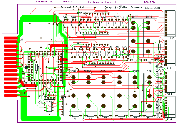 Board Layout